

Graphene is a material comprising a single layer of carbon atoms. It is a superior conductor of electricity -- the unique atomic arrangement of the carbon atoms in graphene allows its electrons to easily travel at extremely high velocity, and its intrinsic two-dimensional geometry opened a promising avenue of research on exploring band structure engineering through manipulating its electrons.
Recently, Pilkyung Moon, Assistant Professor of Physics at NYU Shanghai and a member of the NYU-ECNU Institute of Physics at NYU Shanghai, in collaboration with the research group of Cory Dean from Columbia University, established a robust and versatile technique for band structure engineering of graphene by using an electrostatically defined periodic potential. The research appears in the May 7 issue of Nature Nanotechnology.
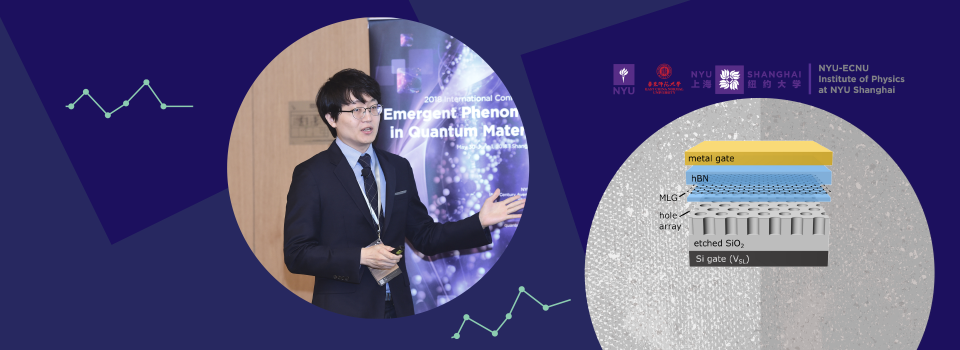
In the research, graphene protected by layers of hBN (a very close isoelectronic match with graphene and a good insulator) is placed on top of the patterned dielectric layer to form square or triangular superlattices. “Our technique allows the electronic structures of graphene superlattices to be controlled in a way that does not disrupt the intrinsic electronic properties of the pristine graphene,” commented Professor Moon.
Through theoretical calculations, Moon revealed the underlying physics behind the technique. He discovered the emergence of new Dirac cones -- the unusual electron transport properties of graphene -- by the superlattice potential and the fractal evolution of energy spectrum. He also revealed the details of graphene’s band structures through analyzing the sequence of the quantized Hall conductivity in a regime where the quantized Hall spectrum evolves into a fractal structure.
“Our results establish a robust and versatile technique for band structure engineering of graphene, bringing graphene one step closer to be applied in today's electronic devices/ quantum computing and communications,” concludes Moon.
The research was partially funded by New York University (NYU) Shanghai (Start-up Funds), NYU-ECNU Institute of Physics at NYU Shanghai, and the NSF of China Research Fund for International Young Scientists granted to Pilkyung Moon (grant no. 11550110177).
Journal Reference:
Carlos Forsythe, Xiaodong Zhou, Kenji Watanabe, Takashi Taniguchi, Abhay Pasupathy, Pilkyung Moon, Mikito Koshino, Philip Kim, Cory R. Dean, "Band structure engineering of 2D materials using patterned dielectric superlattices", Nature Nanotechnololgy, doi:10.1038/s41565-018-0138-7 (2018)